In the field of image processing, various types of research are being pursued, and advanced technology is constantly being developed. The technology demanded by the industry now will be the standard of the future.
The wavelengths of light that people see every day are around 0.4 to 0.8 μm, and this range is called the visible spectrum. Compared to the visible spectrum, the shorter wavelength (smaller number) range is called the ultraviolet spectrum and the longer wavelength (larger number) range is called the infrared spectrum. The infrared spectrum is further divided into the following spectrums
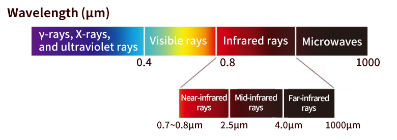 Figure 1: Infrared spectrums
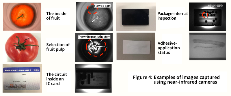
Here, we will introduce efforts related to near-infrared wavelengths, which have characteristics closer to those of the visible spectrum than the rest of the infrared spectrum and have seen increased use in recent years for the purpose of visualizing things that cannot be seen in the visible spectrum, including application for surveillance cameras.
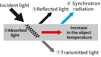 Figure 2: Near-infrared-camera imaging light
In the industrial field, near-infrared wavelengths have long been used for silicon wafer inspections, but in recent years these wavelengths have also been used in a wide variety of other fields, including food, pharmaceuticals, cosmetics (the so-called big three markets), non-destructive inspection of infrastructure, security, biotechnology, authentication, and communications.
Because inspections that use near-infrared wavelengths make it possible to visualize differences in the reflection, absorption, and transmission characteristics of different kinds of light resulting from the composition of the object of inspection, these wavelengths are expected to be introduced in various other fields as well.
Within the near-infrared spectrum, the 1.45-μm wavelength has strong water absorbing characteristics, and there are examples of these characteristics being used to detect water with near-infrared cameras, which is difficult when using image recognition in the visible spectrum.
However, there are also cases where using the 1.45-μm wavelength is difficult, such as when trying to examine the absorption distribution amount of water for an inspection target that has little water overall.
One possible solution is to conduct inspections using the 1.94-μm wavelength, which has even stronger water absorbing characteristics than the 1.45-μm wavelength. Because the water absorption rate of the 1.94-μm wavelength is extremely high, it might be possible to detect the absorption distribution amount in inspection targets that have little water overall, which has not been possible when conducting image recognition inspections using the 1.45-μm wavelength due to a lack of contrast.
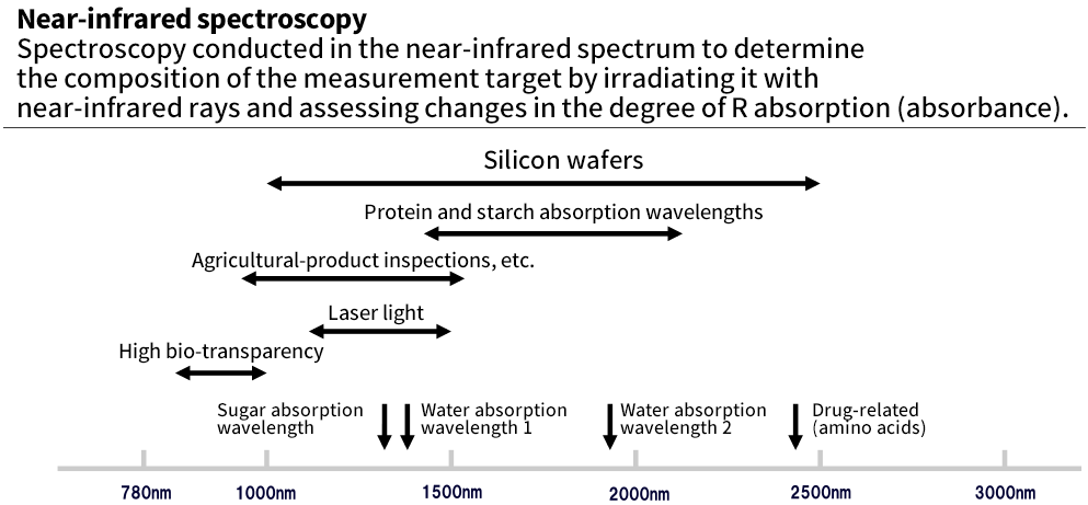 Figure 3: Subjects
In order to achieve inspections using near-infrared wavelengths, it is necessary to understand the different characteristics of light resulting from the composition of objects of inspection, but information related to composition-specific spectral data for the near-infrared spectrum is extremely limited at the present time.
To deal with this situation, the development of hyperspectral cameras, which make it possible to obtain spectral data pertaining to the composition of different substances from imaging results, is currently underway.
Hyperspectral cameras have the ability to simultaneously obtain the characteristics of light (spectrum information) corresponding to two-dimensional position images captured by near-infrared cameras. The data obtained with hyperspectral cameras can be used to gain an understanding of the spectral data associated with each composition. Based on this spectral data, inspection systems that use the most efficient near-infrared wavelengths can be proposed.
To achieve products that are sensitive to the near-infrared spectrum (0.7 to 2.5 μm), which has wavelengths longer than those of the visible spectrum, mixed-semiconductor InGaAS (In: indium / Ga: gallium / As: arsenide) sensors are necessary, and the performance of these sensors is important.
This flow is expected to further accelerate, but in order to effectively utilize the capabilities of near-infrared wavelengths, it is necessary to consider and propose systems that include lenses, lighting, and other components aside from InGaAs sensors. Regarding lenses, because the coating approach and selected material quality can greatly change the characteristics, it is necessary to propose lenses suitable for the target wavelength.
In addition, regarding the lighting, using a halogen lamp makes it possible to utilize a wide wavelength spectrum, but halogen lamps have heat-generation and life-span-related problems. In cases where heat generation, etc. is a problem for a given application, it is likely necessary to also consider the use of an LED light source with the potential to solve the problem.
Therefore, to achieve systems that use near-infrared wavelengths, it is essential to set up an optimal configuration based on consideration of not only the operational situation of the InGaAs sensors (the cooling status, dark current status, etc.) but also the transmittance of the lenses and the amount of light generated by the lighting.
Because the relationship between the InGaAs sensors, lenses, and lighting is extremely important, it is best to propose a complete system that is optimal for the user environment, a task that goes beyond cameras and involves technical cooperation with specialized lens and lighting manufacturers.
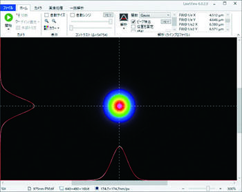
Proposing a single package that includes all the necessary components, including near-infrared cameras and software products that can effectively utilize near-infrared wavelengths, offers users the advantage of being able to immediately introduce a solution.
As a first step toward achieving this, Avaldata Corporation has started selling a package product combining a beam-profiler-dedicated library developed by Kokyo with the ABA-001IR-GE (QVGA / 320 x 256 image / area sensor camera).
This combination of the ABA-001IR-GE and LaseView makes it possible to easily set up a high-functioning, practical beam measurement system that supports the near-infrared spectrum and runs in windows as well as a low-cost beam monitoring system that uses multiple cameras.
The number of cases requiring the near-2-μm wavelength spectrum is also expected to increase for research and development involving the use of laser light.
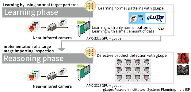
For inspections that use visible wavelengths, because both a lot of high-resolution data and complex, diverse image processing technologies are utilized to achieve object discernment and recognition, it is not easy to link the downstream processing to AI / deep learning.
However, because using near-infrared wavelengths makes it possible to visualize details that were not visible with visible wavelengths by using only a small amount of data, near-infrared wavelengths make it possible to combine downstream image processing with relatively simple operations.
Simplifying image processing is also likely to make it possible to link the processing with AI / deep learning technology, for which a wide range of results is expected.
One advantage of combining these two technologies is the ability to inspect objects that cannot be seen by human eyes with the same level of flexibility as human-based inspections. There is an extremely high level of compatibility between inspections using near-infrared wavelengths and AI / deep learning technology, and collaboration with manufacturers involved in AI / deep learning is expected to help lead to the achievement of specific systems using near-infrared cameras.
In the industrial field, inspections using near-infrared wavelengths are expected to show further advancement. However, to achieve inspection systems that use near-infrared wavelengths, considerations must be based on an understanding of the characteristics of lenses and lighting, and linkage with downstream image processing for which the specific images that can be obtained with near-infrared wavelengths have been considered is also important.
Expectations toward manufactures capable of not only providing near-infrared cameras but also building and proposing complete systems that can take full advantage of the performance of near-infrared wavelengths are likely to increase. (From Avaldata Corporation advertising)

We are an expert group in the field of visual inspections and image processing inspections. We are not just a manufacturer. Instead, we are a visual inspection and image processing inspection system manufacturer that combines knowledge of and experience related to image processing algorithms, optical technology, electronics, and machinery in order to provide comprehensive consulting as a development engineering company.